
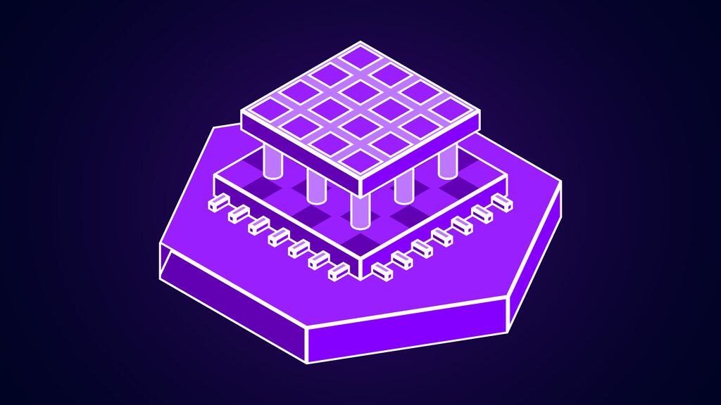
A stacked AI chip developed by researchers at KAIST can tell the difference between a movement that has just happened and the movements that came before it. That sounds simple, but it is exactly what a smartwatch needs to separate a walking stride from a quick swing of the arm. The team did it by stacking two layers of transistors, one that reacts fast and one that reacts slowly, and letting the slow drift of ions inside them act as short-term memory.
The work, reported by Tech Xplore on 28 September 2026 and published in the journal Advanced Materials, uses a solid ion-rich film to set how long each layer “remembers” a signal. The devices told apart all 16 on/off patterns of four pulses, and a simulation built from their measured responses classified videos of moving handwritten digits with over 90% validation accuracy.
This article explains how the stacked AI chip works, why a trick called reservoir computing matters for wearables, what the paper does and does not prove, and how the research fits the wider push to put intelligence on small, low-power devices.
Table of contents
- What KAIST Built: A Stacked AI Chip for Motion Over Time
- Why Motion Is Hard for Small, Battery-Powered Devices
- How the Stacked AI Chip Turns Ionic Delay Into Memory
- Reservoir Computing: The Idea Behind the Stacked AI Chip
- What the Stacked AI Chip Achieved in Tests
- Reading the Paper Against the Announcement
- How the Stacked AI Chip Fits the Neuromorphic Landscape
- From 4-Inch Research Wafers to Smartwatches
- What a Stacked AI Chip Could Mean for Wearables and IoT
- Stacked AI Chip FAQs
- References and Further Reading
What KAIST Built: A Stacked AI Chip for Motion Over Time
For a wearable to distinguish walking from a brief swing of the arm, “it must recognize how movement changes over time”, as the Tech Xplore report puts it. A single snapshot of an accelerometer reading says little. The pattern across a second or two says a great deal.
Two layers with different reaction speeds
The KAIST team stacked semiconductor devices “with different response speeds”, which lets the stacked AI chip “recognize both a change that has just occurred and earlier changes”. One layer tracks the most recent input. The other tracks what has built up over a longer period. Together they give a simple picture of recent history without a separate memory bank.
Who built it
The research was led by Professor Jimin Kwon of KAIST’s Department of AI Systems, working with researchers from UNIST and POSTECH. The paper’s first author is Haksoon Jung, and the ten authors are spread across KAIST’s electrical and chemical engineering schools, UNIST’s semiconductor and energy departments, and POSTECH’s chemical engineering department.
Where it was published
The paper, “Monolithic 3D-Integrated All-Solid Ion-Gated Carbon Nanotube Transistors With Tunable Ionic Conductance for Multi-Timescale Reservoir Computing”, appeared in Advanced Materials on 30 June 2026 under an open Creative Commons licence (DOI 10.1002/adma.202523703). KAIST’s announcement followed three months later.
Why Motion Is Hard for Small, Battery-Powered Devices

Recognising motion is a problem about time, and time is expensive for conventional chips. That is why a stacked AI chip that handles time in its physics, rather than in software, is interesting.
Time is the missing dimension
A photo classifier sees one image. A motion classifier must compare many readings in sequence and weigh recent ones against older ones. In software this is done with recurrent networks or transformers that store past inputs in memory and revisit them at every step. Each revisit costs energy.
The cost of sending data away
A smartwatch could stream raw sensor data to a phone or the cloud and let a larger model decide what it means. That drains the battery through the radio, adds delay and sends intimate health data off the device. Processing the signal where it is measured avoids all three, if the local hardware is frugal enough.
Memory usually costs power
In a digital chip, remembering the last few seconds means writing values to memory and reading them back. The stacked AI chip takes a different route: the memory is a side effect of how the device’s materials respond, so it needs no separate storage step at all.
How the Stacked AI Chip Turns Ionic Delay Into Memory

The core of the device is an ion-gated transistor, in which the current is controlled by ions moving inside a material rather than only by an electric field across a thin insulator.
Ions that are slow to settle
“In these devices, applying a voltage moves the ions within the material and changes the flow of current,” the report explains. When the voltage is removed, “the ions take time to return to their original state.” For a while, the device still carries a trace of the last signal.
That lag “has generally been considered a disadvantage”, because it makes a transistor slow to switch. The KAIST team turned it into a feature. The trace left by earlier inputs is exactly the short-term memory a motion classifier needs, and the stacked AI chip gets it for free from the physics.
From liquid gels to solid films
The main challenge was controlling how long the effect lasts. Until now, such ion-rich materials “have mostly been liquids or soft gels”, which made it hard to fabricate devices precisely or stack them. The team made the material into a solid thin film, a “solid-state ionogel”, with carbon nanotubes forming the transistor channel.
Tuning time constants from microseconds to milliseconds
The team then adjusted two things: the amount of ions in the film and its thickness, which they scaled below a micron. According to the paper’s abstract, that gave “ionic time constants from microseconds to milliseconds”, a spread of about a thousand times. Thin, ion-rich films respond quickly; others respond slowly.
| Feature | Fast tier | Slow tier |
|---|---|---|
| What it responds to | The most recent signal | Signals accumulated over a longer period |
| How it is tuned | Ionic content and film thickness set for a short time constant | Ionic content and film thickness set for a long time constant |
| Range reported in the abstract | Microseconds to milliseconds across the engineered devices | |
| Role in motion recognition | “What just happened” | “What has been happening” |
Reservoir Computing: The Idea Behind the Stacked AI Chip

The paper describes the device as “a compact dual-timescale physical reservoir”. To see why that matters, it helps to know what a reservoir computer is.
A fixed reservoir and a trained readout
Reservoir computing grew out of echo state networks and liquid state machines in the early 2000s. Inputs are fed into a “reservoir”, a dynamic system whose state reflects both current and recent inputs. The reservoir itself is never trained. Only a simple readout layer on top learns to map its state to an answer.
That makes training cheap. Instead of adjusting millions of internal weights, as deep learning does, the system only fits the final layer. The stacked AI chip needs just “a single readout layer” to classify time-varying inputs, according to the abstract.
Physical reservoirs
Because the reservoir is never trained, it does not have to be software at all. Any physical system that responds to inputs in a rich, fading way can serve, from optical fibres to spintronic devices, as a review of physical reservoir computing sets out. The device’s own physics does the heavy computation, which is where the energy savings come from.
Why two timescales beat one
A reservoir with a single time constant remembers roughly one span of history. Real movement mixes fast events, such as a flick of the wrist, with slower rhythms, such as a walking cadence. By stacking a fast tier on a slow tier, the stacked AI chip offers both memories at once. That is the “multi-timescale” in the paper’s title.
A worked example: a stride or a swing?
Imagine a wrist sensor sending pulses to the device. During a walk, similar pulses arrive at a steady rhythm, so the slow tier builds up a high, stable level while the fast tier rises and falls with each step. A single arm swing produces one sharp burst: the fast tier spikes, but the slow tier barely moves because nothing came before it.
The readout layer sees two different combinations of fast and slow states and learns to label them. No step in that process needs a clock, a buffer or a stored history. That is the practical appeal of a stacked AI chip: the history is held in the physics, and only the final decision is computed.
What the Stacked AI Chip Achieved in Tests

The published results cover pattern recognition, a video classification simulation and fabrication at wafer scale.
Sixteen patterns from four pulses
The researchers fed the devices four consecutive input signals, each either on or off. Four binary inputs make 2 × 2 × 2 × 2 = 16 possible sequences, and the devices distinguished “all 16 patterns”. That test matters because some sequences contain the same number of pulses in a different order; only a device with genuine memory of timing can separate them.
Each extra input doubles the number of sequences, which is why longer histories quickly outgrow a single-timescale device.
Moving digits at different speeds
Using the responses measured from the real devices, the team built a simulation of a system that classifies videos of moving handwritten digits. It “achieved validation accuracies above 90% for sequences of moving images played at different speeds”. Classifying video is a classic computer vision task, and playing the same clip faster or slower is a fair test of whether the two tiers capture timing rather than memorising a fixed rhythm. Tasks of this kind echo the Moving MNIST benchmark introduced in 2015, although the report does not name the dataset the team used.
Wafers, flexible substrates and 55 months
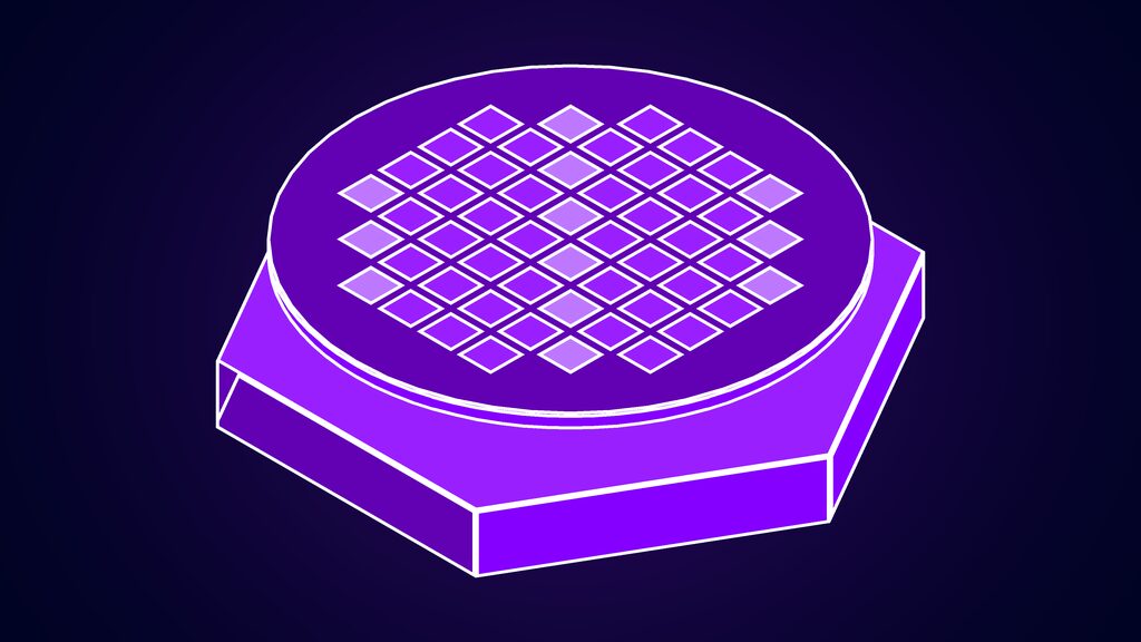
The devices were fabricated on 4-inch wafers and on flexible substrates, and their electrical characteristics “remained stable for 55 months after fabrication”, or about four and a half years. For a stacked AI chip meant for wearables, flexibility and long-term stability matter as much as accuracy.
Reading the Paper Against the Announcement
Press coverage condenses research, so it is worth separating what was shown from what was suggested. The abstract and the KAIST-supplied report agree on the essentials but differ in emphasis.
What the abstract claims
The abstract focuses on materials and device physics: “wide-range engineering of ionic dynamics”, compatibility with “wafer-scale thin-film processing”, and a detailed electrical analysis using impedance spectroscopy. The reservoir demonstration comes in its final sentence, as an application of the device engineering rather than the headline.
A simulation, not a finished product
The motion classification result came from a simulation model built on measured device responses, not from a complete stacked AI chip running a video task end to end. That is standard at this stage of research, but it means the 90% figure depends on the modelling choices as well as the hardware.
The power question is still open
The report is candid: “Further validation is needed to determine how the technology performs, and how much power it saves, in actual smartwatches.” No energy figure for a full motion-recognition system has been published. Claims about battery life should wait for that measurement.
Questions worth asking next
Three questions would sharpen the picture. How does accuracy hold up on noisy accelerometer and heart-rate data rather than digit videos? How much do the time constants drift with temperature and humidity on a wrist? And how many tiers, with how many time constants, would a realistic stacked AI chip need for everyday activity recognition?
| Claim | Evidence published | Status |
|---|---|---|
| Time constants can be tuned from µs to ms | Stated in the abstract, with impedance analysis | Demonstrated on devices |
| Two tiers can be stacked monolithically | Two-tier device described in the abstract | Demonstrated |
| All 16 four-pulse patterns distinguished | Reported from device measurements | Demonstrated |
| Above 90% accuracy on moving digits | Simulation built from measured responses | Simulated, not run on a full chip |
| Stable for 55 months | Reported in KAIST’s announcement | Reported |
| Power savings in smartwatches | None yet | Open question |
How the Stacked AI Chip Fits the Neuromorphic Landscape
The KAIST device belongs to a broad family of research that tries to compute with the physics of materials rather than with ever more digital logic.
Hardware that becomes the network
Earlier this month we covered a review arguing that physical AI could let hardware become the neural network, using self-organising memristive networks. The stacked AI chip is a more engineered cousin: its dynamics are designed and tuned rather than left to self-organise.
Filtering data at the sensor
Another line of work tries to cut energy by discarding useless data early. A National University of Singapore design we reported on uses hardware that filters out irrelevant visual data before it reaches the main processor. Both approaches share a goal with the KAIST work: do less expensive digital computing per decision.
Carbon nanotubes and monolithic 3D
“Monolithic 3D” means the second tier of transistors is built directly on top of the first, rather than made separately and bonded on. It allows dense connections between layers. Using carbon nanotube transistors as the channel, processed at low temperature as thin films, is part of what makes that stacking possible.
| Approach | Where memory of the past lives | What is trained | Main trade-off |
|---|---|---|---|
| Recurrent model on a digital chip | Stored values in memory | All weights | Flexible but energy-hungry |
| Software reservoir (echo state network) | Simulated reservoir state | Readout only | Cheap to train, still digital |
| Single-timescale physical reservoir | Device dynamics | Readout only | Efficient but one memory span |
| KAIST stacked AI chip | Fast and slow ionic dynamics in two tiers | A single readout layer | Efficient, two memory spans; system power not yet measured |
From 4-Inch Research Wafers to Smartwatches
“These devices can be fabricated on large-area substrates using existing thin-film semiconductor processes, and they can also be stacked in multiple layers,” Kwon said. That compatibility is the strongest commercial argument for the approach.
Existing thin-film processes
Many exotic device ideas die because they need a process no factory runs. Thin-film transistors are already made in huge volumes for displays, and the team says its solid ionogel fits wafer-scale thin-film processing. A stacked AI chip that can be printed alongside a sensor, or on a flexible strap, would suit wearables well.
The scale gap
The demonstration used 4-inch (100 mm) wafers, which are research scale. Leading logic fabs use 300 mm wafers, and wafer area grows with the square of the diameter, so each 300 mm wafer offers nine times the area. The chart shows the arithmetic.
What would need to happen next
Before a stacked AI chip reaches a product, the team or a partner would need to integrate sensors and readout electronics, run motion tasks on the hardware itself, and measure the whole system’s power against a conventional low-power microcontroller. Yield and variation across larger wafers would also need to be shown.
What a Stacked AI Chip Could Mean for Wearables and IoT
Kwon says the technology “could be developed into AI chips that analyze movement and physiological signals” for devices that must run on little power, such as smartwatches.
Gait, falls and rehabilitation
Motion over time is the raw material of activity tracking, fall detection and physiotherapy monitoring. Smartwatches already try to detect early signs of illness from such signals. A stacked AI chip that recognises temporal patterns at the sensor could make those features faster and less dependent on a paired phone.
Privacy by staying on the device
Processing a heartbeat or a gait pattern locally means less personal health data leaves the wrist. That helps with data protection obligations as well as battery life, and it reduces the attack surface that cybersecurity teams must defend in connected health products.
What product teams should watch
Teams building Internet of Things (IoT) devices should watch for three signals: a full-system power measurement, a demonstration on real wearable sensor data rather than digit videos, and a foundry or display maker adopting the ionogel process. Until then, conventional machine learning model development on low-power microcontrollers remains the practical route.
Beyond the wrist
Any sensor whose meaning lies in a pattern over time could, in principle, use the same trick. Vibration on a motor bearing, pressure in a pipe and the rhythm of a robot joint are all signals where “what just happened” and “what has been happening” differ. A stacked AI chip printed on a flexible patch could sit directly on such equipment, although the KAIST team has not tested these uses.
Stacked AI Chip FAQs
What is the stacked AI chip from KAIST?
It is a two-tier stack of carbon nanotube transistors gated by a solid ion-rich film. One tier responds quickly to the latest signal and the other slowly to accumulated signals, which lets the device recognise how inputs change over time.
How does the chip remember earlier movements?
Voltage pulses push ions around inside the film, and the ions take time to drift back. Until they do, the device’s current still reflects earlier inputs. That slow recovery acts as short-term memory without a separate memory chip.
What is reservoir computing?
A method in which a fixed dynamic system, the reservoir, transforms inputs into a rich internal state, and only a simple readout layer is trained. Physical devices can act as the reservoir, which saves energy and training time.
How accurate is it?
The devices distinguished all 16 patterns of four on/off pulses. A simulation built from their measured responses classified videos of moving handwritten digits with over 90% validation accuracy at different playback speeds.
Is it a neuromorphic chip?
Broadly, yes. Neuromorphic hardware computes with device physics inspired by the brain rather than with conventional digital logic alone. The stacked AI chip is a physical reservoir, one branch of that field, and it relies on ionic dynamics rather than spiking circuits.
When will it appear in smartwatches?
There is no announced product or date. The researchers say further validation is needed on real smartwatch performance and power savings, and the demonstration used 4-inch research wafers.
References and Further Reading
KAIST Device-to-System Integration Lab: Publications
Recent Advances in Physical Reservoir Computing: A Review
Wikipedia: Reservoir computing
Wikipedia: Carbon nanotube field-effect transistor
Wikipedia: Three-dimensional integrated circuit
Wikipedia: Electrical double layer
Unsupervised Learning of Video Representations using LSTMs (Moving MNIST)
More AI coverage: explore Progressive Robot's AI Models, Tools & Releases hub — hands-on reviews, setup guides and benchmarks in one place.